Ameloot Group
Manipulating Porous Matter
Direct lithography of MOFs @ Nature Materials
Direct lithography of MOFs @ Nature materials
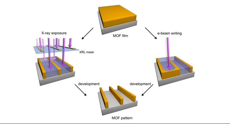
Nanoscale patterning is a fundamental step in implementing MOFs in miniaturized solid-state devices. We developed a resist-free process to pattern MOFs via direct X-ray (DXRL) and electron-beam (EBL) lithography. This process avoids etching damage and contamination yet leaves the porosity and crystallinity of the patterned MOFs intact. Moreover, the resulting high-quality patterns have an excellent sub-50-nm resolution, approaching the mesoporous regime. To demonstrate some of the capabilities of this method, we fabricated a photonic sensor that responds to organic vapors.
This research was carried out in collaboration with VUB (Belgium), TU Munich (Germany), TU Graz (Austria), and Elettra Sincrotrone Trieste (Italy). This work, published in Nature Materials, will speed up the integration of MOFs into microchips.
You may reach us directly for more information, potential collaboration, or industrial partnerships through rob.ameloot@kuleuven.be (Principal Investigator) or bart.vanduffel@kuleuven.be (Innovation Manager).